 |
|

Design Reference
of Internal Oxidation Electric Contact
Tips
1.
Properties of Internal Oxidation Electric
Contact Tips Łş
|
Contact Materials |
FECC NO. |
Properties (Scores 1-9 from
excellent to poor ) |
|
Anti-Erosion |
Anti-Welding |
Electrical
Conductivity
|
|
AgCdO |
D10 |
5 |
5 |
3 |
|
D12 |
4-5 |
4-5 |
3-4 |
|
D15 |
4 |
4 |
4 |
| X2 |
1-2 |
1-2 |
7-8 |
|
X2G |
1-2 |
1-2 |
7 |
| X3 |
1-2 |
1-2 |
7 |
|
NP6 |
1-2 |
1-2 |
7 |
|
AgCdOSnO2In2O3 |
DF15 |
1-2 |
1-2 |
7 |
|
AgSnO2In2O3 |
F11 |
2-3 |
4 |
6 |
|
F13 |
2 |
3 |
6-7 |
|
Remark: Łş |
1. The comparison is made for
above materials only. |
|
2. Above table is for reference
only as switch structures differ from each
other. The design should be made according to
test result. |
| |
|
| 2. Normal
Dimension Tolerance: |
|
|
|
|
| (1). |
The oxidation process will cause
the dimension-change after the contact is
formed. Thus, except Ag layer tolerance is ˇŔ
0.1mm., other tolerances for contact dims. Below
10mm is ˇŔ 0.1mm and for contact dims. Over 10mm
is ˇŔ 0.2mm. |
|
|
|
|
| (2). |
The maximum width, length and
diameter of contact is within 50mm. The limit of
thickness is between 0.7mm~3.0mm.(The thickness
and square measure need to be in direct ratio.)
For special type contact or contact with over
3.0mm thickness, we suggest to produce the
product by powder metallurgy method. Contact
with thickness over 3mm is hard to be oxidized.
|
|
|
|
|
|
|
| (3). |
For AgSnO2In2O3 contacts, the dimension
suggested as below as the material is liable to
be deforming after oxidation process. |
|
|
| |
|
|
F TypeŁş |
Length, Width or Dia. Below
5.0mm: ˇ°tˇ± is better between 0.9mm~1.2mm;
|
|
|
Length, Width or Dia. Over
5.0mm: ˇ°tˇ± is better between 1.2mm~3.0mm
|
|
|
|
|
R Type Łş |
Length, Width or Dia. Below 10.0mm: ˇ°tˇ± is
better between 1.0mm~2.0mm: |
|
|
Length, Width or Dia. Over
10.0mm: ˇ°tˇ± is better between 1.5mm~2.5mm
|
|
|
|
|
Remark: |
The more
contact area is, the thicker the contact
thickness should be to avoid the deforming due
to thickness deficient. |
|
| |
|
|
|
|
|
3. Cambered Surface (
R ): |
|
|
|
| (1)
Cambered surface includesŁş |
|
L ong-side camber, short-side camber and
sphere camber. DonˇŻt use sphere camber to the
|
|
utmost. Sphere camber is hard to
be produced because of its high hardness.
|
|
|
| (2) The
curvature of cambered surface is easily changed
after being heated and oxidized, |
|
Thus, it requires larger
tolerance. The general tolerance is ˇŔ 10R.
| |
|
|
|
|
|
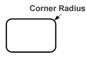
4. Corner Radius ( r ):
|
|
|
The natural formed corner radius after
grinding process of oxidized contact tip is the
first option, other wise the normal permissible
corner radius 0.3r could be adopted. |
 | |
|
5. Brazing Alloy
(Solder Backing): |
|
|
|
| (1)
Cadmium-free brazing alloy such like BAg-5 &
BAg-6 are recommended. But the contacts
|
|
for MCCB could be
brazed with BCuP-5 as MCCB requires less life
cycle than other types of switches. |
|
|
|
| (2) The utility
extent of brazing alloy depends on the contact
area accordingly. (The bigger area |
|
is, the larger utility
extent shall be.) The brazed area should be over
50% of the contact area. After being brazed, the
bonding area should be more 70% of the contact
area. The thickness of brazing alloy depends on
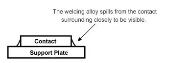
the material properties. After the welding
process, the welding alloy should spills from
the contact surrounding closely to be visible
(the thickness is between1/2 and 1/3 of the
contact thickness). |
|
|
|
|
|
|
| back |
| |
| |
|
Copyright©First Electric Contacts
Corp. Add: jin zhu industrial area ,jiu xiang
villages, qingxi town of Dongguan city,Guangdong,China
TelL:
0769-86811568 Fax: 0769-86811567
Email: mailto:postmaster@fecc.net.cn |
|